Page Title
Scanning Electron Microscopy
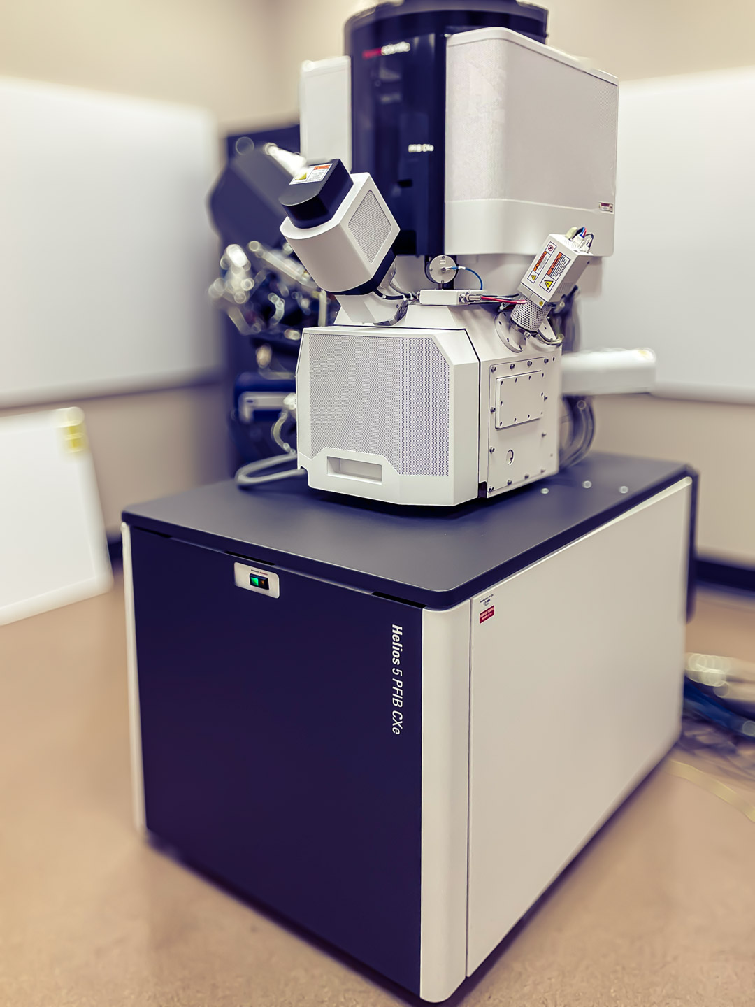
ThermoScientific Helios G5 CXe Plasma FIB/SEM
The Helios 5 is a DualBeam focused ion beam microscope (FIB). It has an electron column for ultra-high-resolution scanning electron microscopy (SEM) tasks and a xenon (Xe) plasma ion column for sample preparation for TEM and atom probe tomography (APT), as well as for 3D characterization of materials.
Use of the Auto Slice & View software in combination with our Oxford Instruments Ultim®Max energy dispersive X-ray spectrometer (EDS) and/or Oxford Instruments Symmetry® Electron Backscatter Diffraction (EBSD) detector allows fully-automated multi-modal materials characterization workflows.
- Available detectors:
- in-lens SE/BSE detector (TLD)
- Everhart-Thornley SE detector (ETD)
- in-chamber electron & ion detector (ICE) for secondary ions (SI) and electrons (SE)
- retractable STEM 3+ detector (BF/DF/HAADF segments)
- Flexible 5-axis motorized stage:
- tilt range: -15° to 90°
- max. weight: 500g in any stage position, 5kg at 0° tilt
- Oxford Instruments Ultim®Max energy dispersive X-ray spectrometer (EDS)
- Oxford Instruments Symmetry® Electron Backscatter Diffraction (EBSD) detector
- MultiChem™ Gas Injection System (GIS) for Pt, W and C deposition
- EasyLift™ NanoManipulator for in situ sample manipulation
- Auto Slice & View for 3D material characterization by FIB serial sectioning and analysis using EBSD and/or EDS, followed by advanced 3D visualization with the Avizo™ software available on our data processing and analysis workstation
- AutoTEM for automated TEM specimen preparation
- iFast Developer software for creating individual FIB/SEM automation workflows
Resolution
- Electron beam: 0.6 nm at 30 kV (STEM)
- Electron beam: 0.6 nm at 15 kV
- Ion beam: 4.0 nm at 30 kV (preferred statistical method)
- Ion beam: 2.5 nm at 30 kV (selective edge method)
Beam parameters
- Electron beam current range: 0.8 pA to 176 nA
- Electron accelerating voltage range: 200 V – 30 kV
- Ion beam current range: 1 pA – 100 nA
- Ion beam accelerating voltage range: 500 V – 30 kV
FEI Quanta 3D FEG FIB/SEM
The Quanta™ 3D DualBeam™ FEG FIB-SEM combines a Focused Ion Beam (FIB) with a high-resolution Field Emission Gun Scanning Electron Microscope (FEG-SEM). This combination provides enhanced 2D and 3D materials characterization and analysis for a wide range of samples.
A focused Ga Ion beam allows for micro and nano-scale cutting of material during TEM sample preparation, EBSD surface milling, and automated milling scripts for micro-pillar patterns. Additionally, the FIB provides a “slice and view” technique that allows for 3D reconstruction of a sample, providing the ability to image and analyze subsurface features. Featuring three imaging modes – high vacuum, low vacuum and ESEM, it accommodates the widest range of samples of any SEM system.
The Quanta 3D FEG’s novel, field-emission electron source delivers clear and sharp electron imaging and increased electron beam current enhances EDS and EBSD analysis.
The integrated EDAX Pegasus EDS & EBSD system brings new capabilities and flexibility to engineers and researchers needing chemical composition analysis, element distribution, crystallographic orientation, grain size and distribution etc.
- High-resolution SEM imaging with environmental control
- Specimen etching or deposition
- Precise circuit modification/nanofabrication
- Micro/nano-scale patterning
- TEM sample preparation by combining FIB milling and Omniprobe lift-off process
- Elemental analysis and mapping
- Crystallographic analysis and mapping
- Field emission electron source with probe current adjustable up to 36n
- Beam acceleration voltages: 500V-30KV
- High vacuum, low vacuum and ESEM imaging mode
- Spatial resolution: 1.3nm in secondary electron imaging and 1.7 in ion beam imaging
- Motorized 5 axis specimen stage
- Solid state backscattering electron detector
- EDAX Pegasus EDS/EBSD detectors
